New Innovative Way to Functionally Verify Heterogeneous 2D/3D Package Connectivity
This paper introduces a new way to functionally verify packaging connectivity using formal verification that can exhaustively verify all interconnections between IC blocks. The flow is automatic for all steps, from creating connectivity specifications to verifying packaging output connectivity. The automatic parallel algorithms on the compute grid can verify huge numbers of connections in minutes or even seconds. The script for the flow is simple and only takes a few minutes to set up.

-
Introduction
Historically IC package design has been a relatively simple task which allowed the die bumps to be fanned out to a geometry suitable for connecting to a printed circuit board. The package netlist was often captured by the package designer, typically using Excel to manually assign net names to the desired die bumps and BGA balls to achieve the intended connection.
Modern package and interposer design has become a system integration task: designers have the responsibility to take input from various stakeholders – who are often designing their content at the same time the package or interposer is being designed – and create a design which is both electrically and physically correct and functions as designed.
For the purposes of this paper, the term “substrate” will be used to generically represent both the package and interposer designs. For many design and verification tasks, the target implementation of either the package or interposer can be used interchangeably, as the design task and verification tasks are similar despite the differences in manufacturing technology and implementation tools.
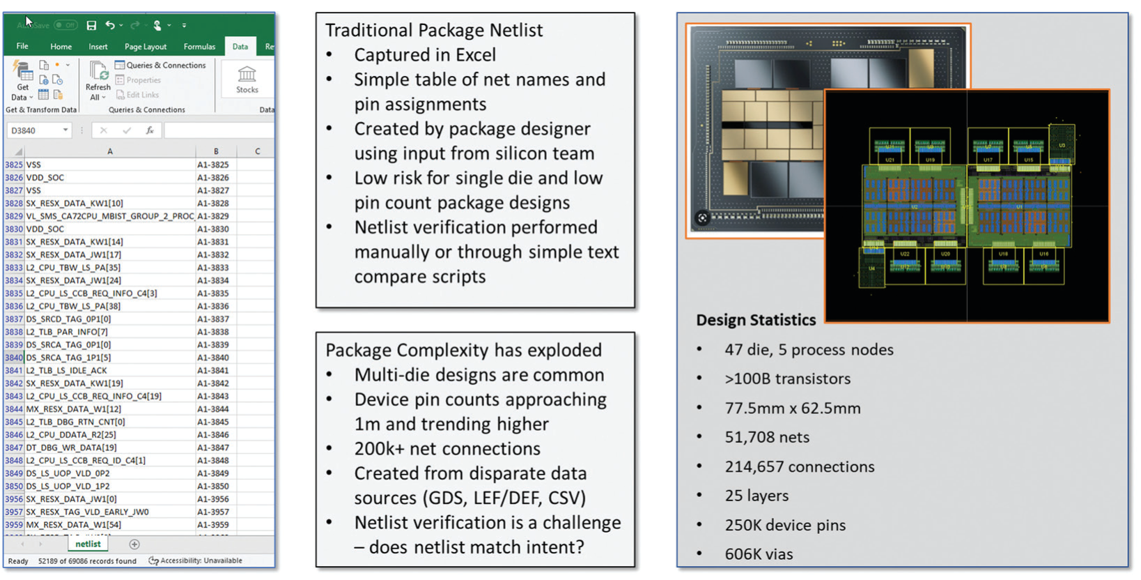
Figure 1. History of IC package design
Challenges
With rapid advances in package technology and the explosion of AI and high-performance computing applications, substrate designers face design challenges that are breaking their existing methodologies. Designs with 500,000 bumps and several hundred thousand connections are becoming commonplace. With hybrid bonding technology promising millions of bump connections, a spreadsheet is no longer capable of managing the complex connectivity. Heterogeneous integration has brought with it some challenges for the package designer. The source data is being supplied in a myriad of data formats:
- Ball map CSV files
- LEF/DEF from place and route tools
- GDS
- Verilog RTL
- Spreadsheet data
- Plain text files
As each component of the design is introduced, it must be connected to the other components in the system. Spreadsheet based design requires that every connection be defined as a scalar. One can quickly see how it would become tedious and error prone to attempt to define the connectivity one bit at a time in high bandwidth memory (HBM1) based design, with its 1024-bit width.
To handle the explosion of die-to-die connections, substrate designers are beginning to embrace language-based design to define the connectivity of the system. It is far more efficient and less error prone to write Verilog RTL using proper bus notation to connect the various components of a system together than it is to either define connectivity one bit at a time in a spreadsheet or develop specialized Excel macros to populate a connectivity table.
-
Download Paper
-
New Innovative Way to Functionally Verify Heterogeneous 2D/3D Package Connectivity
Formal Verification Jan 16, 2026 pdf
-