How Microsemi Uses Questa Formal Connectivity Check to Improve Quality and Productivity
The complexity of our SoCs continues to grow at a furious pace, with a corresponding increase in the integration of more functionality using a massive number of IPs, in addition to the overlay of BIST, multiplexing of I/Os, and other "out of band" circuitry. This complexity makes manual verification of IP integration too risky, time consuming, and error prone.

-
Overview
The complexity of our SoCs continues to grow at a furious pace, with a corresponding increase in the integration of more functionality using a massive number of IPs, in addition to the overlay of BIST, multiplexing of I/Os, and other "out of band" circuitry. This complexity makes manual verification of IP integration too risky, time consuming, and error prone.
Even small errors in signal naming conventions, incorrectly port mapped bit positions, and other fault conditions can lead to confounding bugs that can waste many man-hours debugging the SoC/block functionality; let alone the risk of an expensive device re-spin if these bugs escape.
Our overall verification flow uses a three-pronged approach, using simulation, emulation, and formal. Our primary goal is to find and fix bugs as early as possible. This goal is of such important because as we progress in the timeline of any project the cost of fixing bugs grows exponentially. We want to save time and save budget by using the right tool for the right problem. For connectivity issues, we have successfully used formal verification at all levels of SoC development: block, subsystem, and full chip.
We will share how we employed the formal-based Questa Connectivity Check App to eliminate risks, improve quality, and increase productivity. We will also provide some results of a case study that shows how we were able to verify the connections for a complex SoC having 300K+ gates, 530+ IOs, conditional connectivity, and power ports. The Questa Connectivity Check App helped us find bugs at early stages of our project and shortened our time-to-market.
The SoC Connectivity Verification Challenge
The chips that the Microsemi SoC Division designs have a large number of I/O pads and a large number of internally and externally designed IP that need to be connected. Verification of this SoC connectivity has become a very challenging, high-risk task.
Even small SoCs have multiplexing of I/Os, inserted BIST, tens of thousands of static and dynamic interconnections, and low power isolation circuitry — all layered on top of the baseline point-to-point interconnects. As if that weren't difficult enough, both legacy and third-party IP are often under-documented. Beyond these "initial" challenges, we have to be able to account for the constant stream of bug fixes and ECOs throughout a project's life cycle.
All this adds up to the need to have very good verification of the connectivity. We want to eliminate the connectivity related bugs as soon as possible, both because it's easier to find and fix them earlier and we do not want to deal with them in simulation and emulation.
Formal Advantages
The increasing complexity of IP makes it pretty much impossible to integrate them correctly without formal tools. We have done connectivity verification with simulation, but it has several disadvantages compared to formal technology. Simulation requires the high overhead of creating a testbench and tests.
The simulation will be as good as the test that you write. You have to make sure you've created the right tests to go into the right corner cases, and you have to make sure that you've done enough verification with those tests. The time to find bugs can be too long, followed by a long process of fixing them and validating those fixes. No matter how smart and thorough a job you do, it's difficult to cover all the cases.
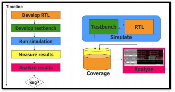
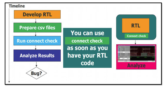
Figure 1. A simulation flow, on the left, requires more effort, more steps, more time and has lower corner case coverage than the Formal Connectivity Check app flow, shown on the right.
This is perhaps the biggest advantage of the Questa Formal Connectivity Check app over simulation: formal analysis is exhaustive. Formal considers all modes of operation and is much better at catching corner case scenarios.
Another advantage of formal verification is that the apps work without needing any kind of a testbench. Set up is quick and easy. As soon as the RTL is ready you can just run the formal. And it's much faster than simulation. Runtimes are much shorter, and it doesn't have to run more and more tests to hit all of the corner case scenarios — it takes only a single formal run.
A significant advantage is that assertions are automatically generated. The need to know an assertion language and the assertion-based verification methodology is very much reduced with the formal apps. You can review the assertions, but you do not have to write them, and you do not have to debug them for syntax errors.
Formal apps also make it easier to debug using waveform counterexamples, as any mismatches between the specification and the DUT are flagged. Finally, bug fixes and revalidation are very fast. Once you've identified and fixed the bug, it is just a matter of getting the new RTL or the new spec, depending on what was wrong initially.
A Formal-Based Connectivity Verification Flow
The Microsemi connectivity verification flow automates both assertion creation and formal analysis of assertions. It has has two inputs: the RTL code and the connectivity spec. These are fed into the assertion generation utility which uses them to automatically generate the connectivity assertions. These are fed along with the RTL into the Questa PropCheck tool, which performs automated formal analysis to verify whether the generated assertions are true or not for the RTL.
If an assertion fails, the tool immediately outputs counterexamples so we can see the errors. It's straightforward to get the counterexamples and debug the waveforms. Also, in parallel, the flow generates a USDB coverage database and creates a test plan. The test plan is used to track progress in the Questa Verification Management tool.
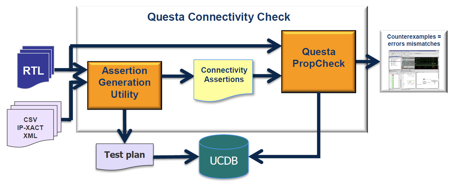
Figure 2. Microsemi SoC Division connectivity verification flow.
Connectivity Check Case Study
We used the Connectivity Check ap to verify connectivity at the block, subsystem/cluster, and full chip levels. As well, we used it to check the connectivity of approximately 600 I/O ports. An interesting aspect is that this involved checking connectivity from a lower level subblock written in RTL to higher-level analog portions of the block that were hand-designed.
First, we set up the flow environment, which is fairly simple to do, and prepare the connectivity specification. We used the CSV format, but the tool also supports XML and IP-XACT. Then we go through the typical process of run, verify the results, debug, fix, and iterate.
Eight Steps to Verify Connectivity
There are eight steps in the connectivity check flow itself.
Step 1: We compile the design. This is normal stuff.
Step 2: The tool automatically generates the connectivity assertions. In this second step three things are generated: two SV files (the checkers and the bind file) that we're going to use later, and the test plan, which is an XML file that shows all the assertion.
Step 3: The checkers and the bind files are used to compile the connectivity assertions.
Step 4: Formal analysis is run for the connectivity check.
It is good practice to have an INIT sequence and to have directives so the tool will run with better performance. They INIT sequence show what the reset signals are and how many cycles are needed to hold the reset at the beginning of the run. The directives show information about the clock signals. It is also good practice in the directives to black-box any blocks that are not needed during the connectivity check, especially for large analog blocks. By black-boxing as much logic as you can improves compile and run performance at the subsystem and full chip levels.
It is also helpful for this or any new verification flow to run a very small number of test cases with known results to make sure that the tool passes where it should and fails where it should. This allows you to know that you went through the hierarchy correctly and ensures that everything will go more smoothly when you do your actual verification.
Step 5: The UCDB and the XML test plan are generated in the needed format to create the connectivity test plan. This is a good place to use the prefix to actually show the hierarchy, so that the tool will run properly.
Step 6: Update the connectivity test plan. Here we merge the coverage results with any other assertions and coverage data that we already have in the test plan for the DUT.
Step 7: We review the test plan and coverage data. Basically, we look in the coverage to make sure that everything is 100% covered.
Step 8: Use qverify to query the debug database that has been generated. If an assertion has failed, you debug the failure. If coverage has not been made, you debug the coverage. In general, there is one-to-one correspondence: if a connectivity assertion fails, then coverage will not be made, so you will probably start with debugging the assertion failure.
Interactive Debug with the Questa Verify GUI
For debugging, we use the Questa Verify (qverify) debug windows. The qverify GUI is very valuable for debug. It shows the source code, the waveforms, and counterexamples. We can also see the schematic and the properties. Good properties are shown in green (as all the properties are in Figure 3, lower left corner); failing ones would be shown in red to indicate a violation. We can double click on a property that failed and the tool opens up the waveform and the schematics, so we can see the source code, making it easier to debug.
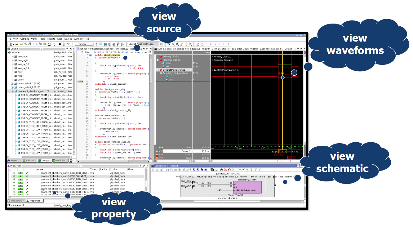
Figure 3. With the Questa QVerify GUI, waveforms take you right to the root cause.
It is important to track and debug missing coverage to ensure completeness. The Covergroups window in Figure 4 clearly shows where assertions are failing. In this case, three of the assertions failed, so they show as not covered. This makes is easy to locate and debug the assertions to make sure your coverage is 100%.
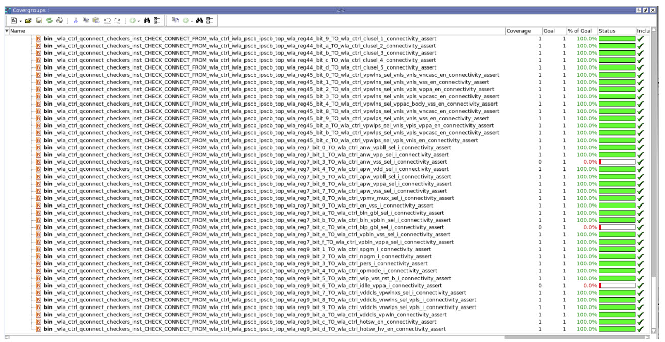
Figure 4. The Questa Covergroup window shows missing coverage.
Results: Showstopper Bugs Squashed
We had very good results using the Questa Connectivity Check app. It found multiple showstopper bugs, including:
- Source connected to the wrong destination
- Source connected to destination with scrambled bits
- Breaks in connectivity, missing connection
Some of these bugs could be found with a testbench and tests, but it's much more difficult. One of the big advantages of the formal tool is that it is much more straight forward.
We also found issues in the analog domain. At the full chip level there was a bug found by the formal tool, whereby two analog sources were driving the same destination. We were told it's okay to have this connectivity, but we couldn't have both analog sources enabled at the same time. So, physically they are connected, but they cannot drive at the same time. And because we have a number of variants on the product that we're doing now, we find this again and again, so this was an important find by the Questa Connectivity Check app tool.
Conclusion
In conclusion, we really want to find bugs early. We want to use the right tool, at the right time. Formal is indispensable for these directives because it is exhaustive, and it reaches into all corner cases.
Simulation alone is not good enough for today's connectivity checking projects, for several reasons:
- Too long to set up
- Long run time
- Hard to find bugs, easy to miss bugs
- Not exhaustive
On the other hand, the formal based Questa Connectivity Check app is exhaustive and more productive:
- Easy to set up — no knowledge of formal is necessary
- Run time is shorter — depending on DUT size
- Easier to debug failures
- Automated assertions — you don't need to be an expert in assertions
- Exhaustive results
- Automated test plans enable progress tracking and regression
The bottom-line is that the Questa Connectivity Check automated, formal-based app supports Microsemi's philosophy of finding bugs as efficiently and early as possible.
-
Customer Profile
-
Customer Profile
Headquartered in Aliso Viejo, California, Microsemi® offers a comprehensive portfolio of semiconductor and system solutions for aerospace and defense, communications, data center, and industrial markets.
The Microsemi SoC Division develops and produces FPGA and ASIC designs.
Verification Pain Points
- Increasing SoC complexity makes connectivity verification a high risk, highly challenging project
- Testbench verification of all static and conditional connections is time consuming and error prone
- Need to eliminate connectivity related bugs as soon as possible, because it is easier to find and fix them earlier
Formal Connectivity Check App
- Found multiple showstopper bugs, including in analog domain
- Much better than simulation at catching corner case scenarios
- Easy to set up — no knowledge of formal is necessary and no testbench is required
- Run time is shorter
- Easier to debug failures
- Automated assertions — expertise in assertions not required
- Exhaustive results
- Automated test plans enable progress tracking and regression
-
Microsemi

-