Design for Test Verification
As semiconductor devices become increasingly complex and diverse, spanning automotive, AI/ML, 5G, and heterogeneous 3D-IC designs, Design-for-Test (DFT) verification plays a crucial role in ensuring not only high-test quality but also seamless integration with system-level requirements. While test insertion flows such as scan insertion, BIST/MBIST integration, and boundary scan logic have matured to deliver cost-effective, scalable test solutions, DFT verification remains a bottleneck that demands significant attention.
-

On-Demand
Tackling Emerging DFT Verification Challenges with Questa One
In this webinar, you will learn how the Questa One DFT Verification solution, combined with Tessent Silicon Lifecycle Solutions delivers an evolution in user experience and performance to address emerging verification challenges.
-

On-Demand
Enhancing Defect Coverage in DFT with Functional Fault Grading
In this webinar, you will learn how functional fault grading enhances defect coverage and the key advantages of integrating functional fault grading into DFT processes, specifically addressing faults untestable by scan tests.
-
Industry Challenges in DFT
Engineers and organizations are grappling with the challenges brought on by technology scaling, design scaling, and system scaling, making traditional verification approaches insufficient.
Technology Scaling
As semiconductor technologies advance toward smaller process nodes, a number of critical challenges arise. Shrinking geometries lead to higher defect densities, increasing susceptibility to manufacturing flaws and long-term reliability concerns. At the same time, process variations become more significant, introducing variability in device performance and behavior. Moreover, subtle defect mechanisms, such as internal cell faults and latent failures, are increasingly difficult to detect using conventional fault models. Aging effects and wear-out mechanisms also become more impactful, further complicating efforts to ensure robust and reliable silicon.
Design Scaling
Modern semiconductor devices comprise billions of transistors and frequently integrate numerous heterogeneous IP cores, significantly increasing the complexity of DFT implementation. The widespread use of diverse IP and increase in number of unique cores result in larger volumes of test data and extended test durations, escalating both the cost and intricacy of test operations. Furthermore, power management during testing becomes a critical concern, as the application of dense test patterns can lead to power spikes that compromise test accuracy or, in extreme cases, risk damaging the device.
System Scaling
As demand grows for ultra-high reliability, especially in mission-critical domains such as automotive, aerospace, and high-performance computing, the scope of Design-for-Test (DFT) has expanded to encompass the entire product lifecycle, from initial manufacturing through to end-of-life operation.
In the early stages of a device’s life, more sophisticated and comprehensive fault models are now essential to capture a broader spectrum of potential defects, including those stemming from process variation, aging effects, and environmental stressors. These models must go beyond detecting traditional manufacturing faults to also identify latent defects that may emerge only after prolonged use or under specific conditions.
To meet the expectation of sustained, fault-free operation over many years, modern systems increasingly rely on dedicated hardware and embedded diagnostic logic to monitor silicon health in real time. This in-system monitoring enables the detection of degradation and emerging faults during normal operation, allowing for proactive intervention to maintain system integrity and extend device longevity.
Tessent™ Silicon Lifecycle Solutions deliver industry-leading, scalable, and cost-effective solutions designed to meet the evolving challenges of DFT in advanced semiconductor designs. Its comprehensive portfolio enables seamless integration of test technologies across the entire product lifecycle, from manufacturing test to in-system diagnostics, ensuring high fault coverage, optimized test time, and minimal overhead. Tessent’s advanced ATPG, compression, and fault modeling capabilities are engineered to tackle complex defect mechanisms, while its embedded analytics and in-system test solutions support real-time silicon health monitoring for mission-critical applications. With a modular architecture and automation-driven workflows, Tessent empowers design teams to efficiently tackle the elephant in the room, delivering DFT at scale and reducing cost and time-to-market without compromising quality or reliability.
It's important to not ignore the baby elephant in room, and that is the verification activities required to reach DFT-sign off. The combination of factors across technology scaling, design scaling, and system scaling have created a perfect storm for DFT verification, driving the need for solutions that are scalable, integrated, and future-proof.
DFT Verification Challenges
As semiconductor designs scale in complexity, DFT verification presents growing challenges at both the core and top levels. Following test IP insertion, such as scan compression, on-chip clock controllers, and MBIST/BISR, rigorous post-insertion verification is required to ensure no functional issues have been introduced. This includes equivalence checking between pre and post insertion RTL and careful handling of synchronization, especially across clock and reset domains. Common pitfalls like improper signal synchronization, reconvergence glitches, and memory corruption due to metastable resets must be addressed early to avoid costly downstream debug.
At the core level, ATPG pattern verification involves a significant volume of both parallel and serial simulations across multiple configurations, timing corners, and fault models. As each core undergoes block-level verification, the workload grows exponentially with the number of unique cores. When these cores are integrated at the top level, further verification is needed to ensure retargeted patterns function correctly in the full-chip context. The scale and complexity of this process demand robust and scalable verification methodologies to achieve DFT sign-off efficiently.
System-level scaling introduces two major DFT verification challenges. The first is achieving the high defect coverage required by reliability-critical markets such as automotive and aerospace. Structural scan testing alone may not meet these stringent requirements, prompting teams to explore additional coverage from test setup procedures and functional pattern supplementation. Measuring and closing the residual coverage gap is now a key engineering focus.
The second challenge involves pre-silicon verification of in-system test (IST) infrastructure. This includes validating both the accurate delivery of test pattern payloads to the test network and the correct processing of captured data for defect detection. Since IST relies on both hardware and software components, robust hardware/software co-verification is essential to ensure end-to-end correctness and diagnostic reliability during in-field operation.
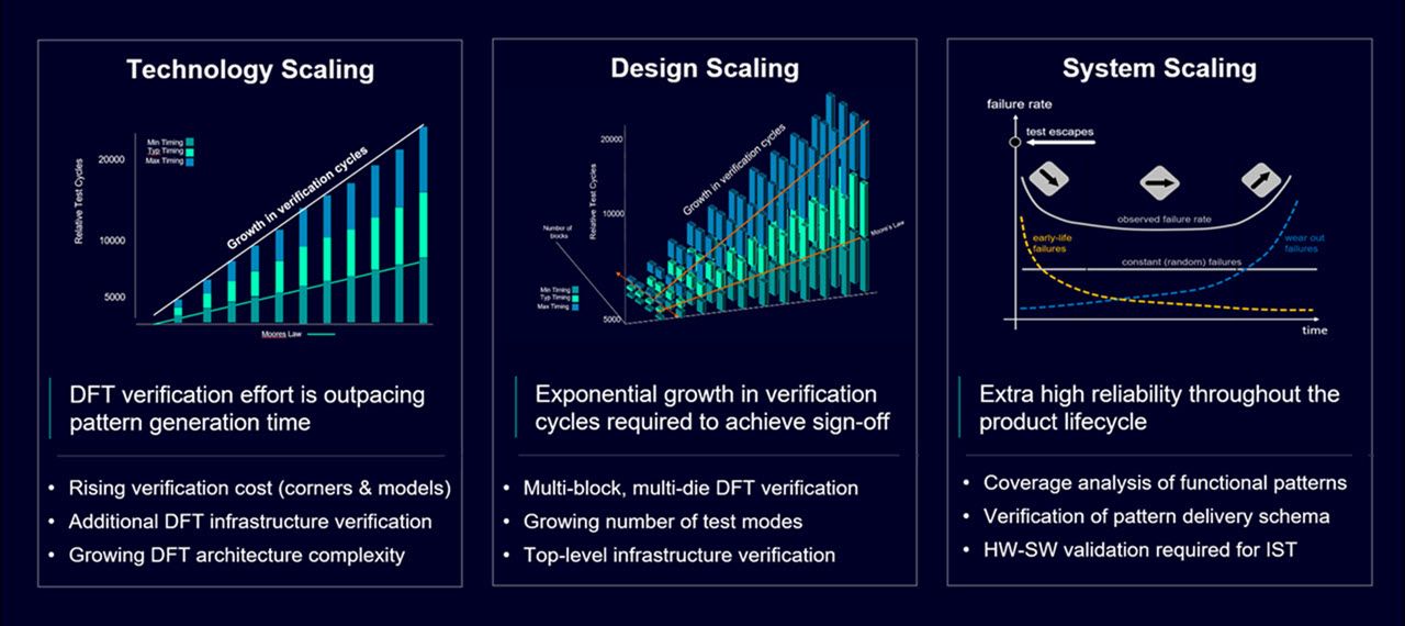
Figure 1. DFT verification challenges across technology, design, and system scaling
-
Questa One DFT Verification

- 0:00
-
Questa One DFT Verification - Content
The Questa™ One DFT Verification solution is a powerful, comprehensive suite of technologies designed to address the challenges of technology scaling, design scaling, and system scaling in DFT verification. By integrating seamlessly with Tessent Silicon Lifecycle solutions, Questa One provides a unified platform that connects verification workflows to the entire DFT process. This integration ensures efficient collaboration, streamlined workflows, and a holistic approach to DFT verification activities.
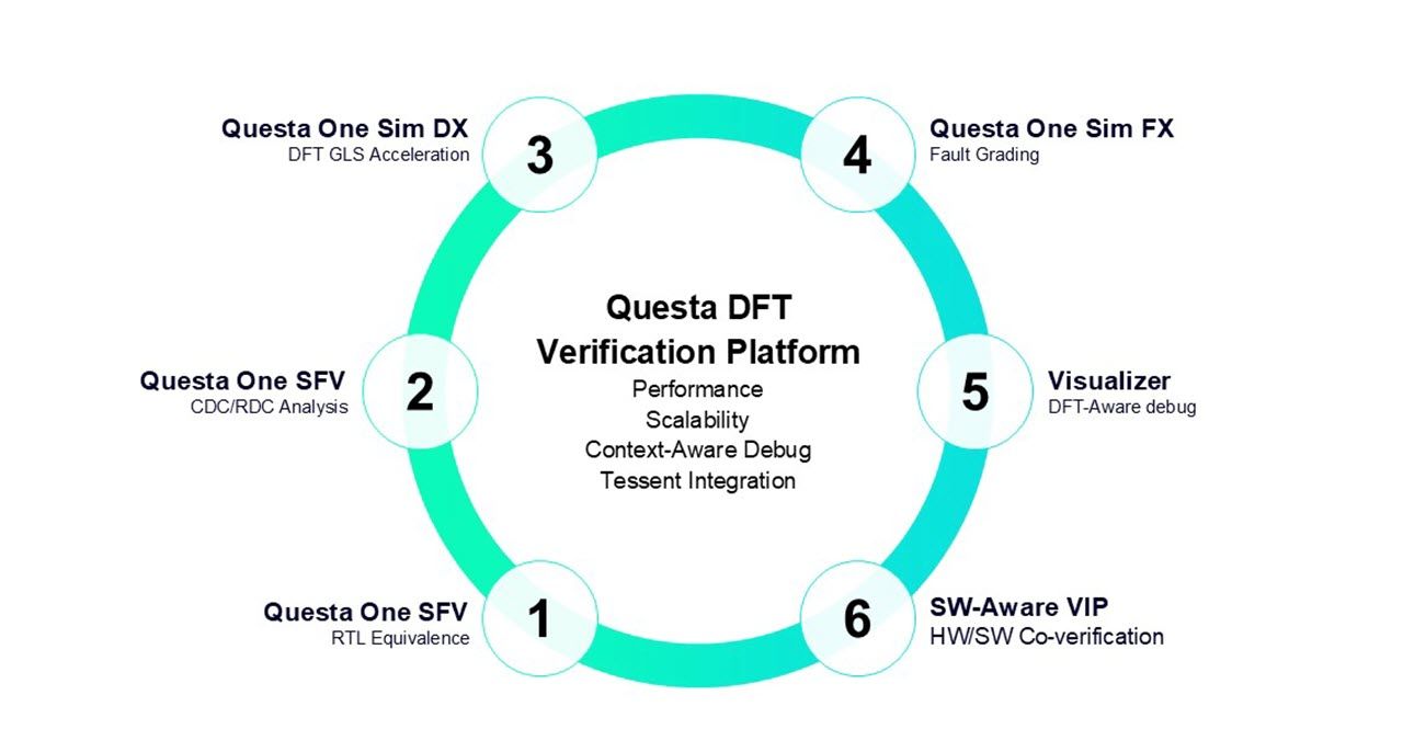
Figure 2. Questa One DFT Verification Solution
Comprehensive Features and Capabilities
The Questa One solution offers a diverse set of capabilities to enhance the efficiency and effectiveness of DFT verification. Key features include:
- Gate-Level Simulation Enhancements: Improved performance for gate-level simulations delivering industry leading performance and productivity.
- Static Analysis: Post insertion equivalence checking to validate functional correctness.
- Automated Directives: Seamless metastability analysis following MBIST insertion.
- Protocol SVA Generation: Automated SystemVerilog Assertion generation for glitch scenario analysis.
- Functional Fault Grading: Scalable fault simulation to measure defect coverage from functional patterns.
- DFT-Aware Debug: Advanced debug capabilities, including X-propagation analysis.
- Software-Aware Verification IP: Accelerated in-system test (IST) hardware/software co-verification.
Accelerated Runtime Performance
A standout feature of the Questa One solution is its exceptional runtime acceleration. Leveraging advanced DFT-aware techniques and optimizations, it delivers significantly faster verification performance across various DFT tasks. This acceleration reduces verification time, enabling design teams to meet tight project deadlines, improve productivity, and accelerate time-to-market. The platform complements typical Tessent DFT implementations by providing layered assurance throughout the lifecycle, ensuring reliability and quality in every step.
Integrated Ecosystem
The Questa One solution is fully integrated with Tessent lifecycle tools, enabling design teams to verify DFT implementations efficiently. This integration provides a robust framework that supports the entire DFT lifecycle, from early DFT insertion to final sign-off.
By reducing verification runtimes and enhancing workflows, the solution ensures that teams can achieve DFT sign-off efficiently and meet tight project schedules.
-
Learn more about the Quest One DFT Verification Solution
-