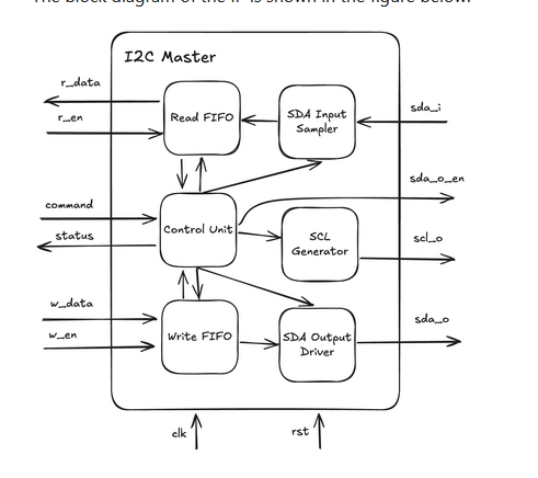
I came across a design on GitHub and wanted to verify the design on my own. The Design has a master slave config as shown below.
MASTER -
SLAVE -
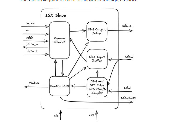
My confusion is about the I2C interface for master and slave.
Now I want to verify it by making two separate interface for FIFO and memory side and two different interface with i2c_master and i2c_slave and then write agents around them to verify but I am confused with i2c interface on how should I go ahead with verifying the master_i2c as apart from sda_i every other signal is output. Also, would it be wiser to adapt to one interface for both of them(i2c)?