Read values are wrong in UART Verification

Dear Everyone,
I am currently implementing an UART verification project using SystemVerilog. In this particular design the transmitter and receiver communicate using a separate baud clock made from original clock and baud rate. The closest architecture is shown in the below image. I have observed that the write values are fine after reset whereas read values are wrong as they display the values which are from its previous cycle. The code is here. I believe the issue is with the synchronization with the monitor why because when I tried separately the UART receiver with a simple verilog testbench, it functions properly and the code for that is here. One more thing is that EDA playground is limiting the simulation period due to some issue. I kindly request you to help me in fixing this read value issue.

Architecture:
The architecture is the final system, but currently I am doing a smoke test where I check onething at a time like a read, a write or a reset.

Error Screenshot:
The error output is below. I am sending 95 from driver for a read test but I am receiving 190 which is the 7th cycle value but not the 8th cycle value (which is actually expected)

.

Monitor Code block:
The problematic monitor code block is below. I was trying to add/remove some clock cycles here which is altering the values I see but unable to fix the issue.

 //read [idle -> start(1 cycle) -> data(8 cycles) - >stop(1 cycle) ]

      else if(intf.rx == 1'b0)begin // from idle to start state in a receiver
        mon_tr = new(); //create a transaction class object and assign the operation as read
        mon_tr.oper = READ;
        data_rx = 0;  //temporary storage
        @(posedge intf.uclkrx); //cycle delay given for data state
        wait(intf.rx_done == 1); // wait until it goes to stop state
        @(posedge intf.uclkrx); //cycle delay for debigging, now extract the received data from dut
        data_rx = intf.rx_data;  // put the received data in the temporary storage
        mon_tr.data_rx = data_rx; // update the transaction object value and send it to scoreboard for checking the correctness
        mon2scb.put(mon_tr);end //it is the mailbox for monitor and scoreboard communication

I’ve taken a quick look at the link you provided and… it’s a lot of code!

To make it easy for people to help you (and possibly to find the problem yourself), I suggest you try something like the following:

  • Check you are seeing behaviour that looks “wrong” with your example.
  • Add any relevant debug prints that you think will make things obvious (and comment out any other prints)
  • Reply to this question with a snippet of the output that shows the problem, together with an explanation of what’s wrong with it.

That might well be enough to make it clear what’s going on. In particular, it sounds a lot like something isn’t picking up (non-UVM) “sequence items” properly for read transactions in your monitor.

My first thought when glancing at the code was slight surprise. The diagram you’ve pasted looks like the tx and rx paths are essentially parallel. The code in your monitor can only support one direction on any given cycle. Is that what you intend? (Also, the “repeat (10)” is quite a red flag for a monitor that I’d normally expect to run forever)

Dear Rswarbrick,

I have updated the question accordingly. Coming to your architecture related question. Currently I am doing a basic smoke test, like a read, a write , a reset. After proper working I will be testing simultaenous read and write functionality. Kindly let me know if still more clarity is needed.

Thanks for the answer. I spent a bit of time working through the code, tweaking things in a copy as I read. I thought it might be helpful to leave “review comments” as I go, so I filled this out (there’s a link to what I ended up with at the end).
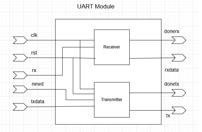
The design code:

  • With my background in ASIC design, I started switching stuff in design.sv to use asynchronous reset assertion, before realising this is probably targeting an FPGA. I’d probably recommend switching over anyway: it will still work on an FPGA and is possibly a bit more conventional. (always @(posedge clk or posedge rst))
  • Rather than using a 32-bit counter for the clock division, you probably want something smaller. It also doesn’t need supplying from the testbench. Maybe something like this?
  // The main clock is divided down to a uart clock with a posedge every clock_freq / baud_rate
  // cycles.
  localparam int unsigned CountMax = (clock_freq / baud_rate / 2) - 1;
  localparam int unsigned CountWidth = $clog2(CountMax);

  logic [CountWidth-1:0] count;
  always_ff @(posedge clk or posedge rst) begin
    if (rst) begin
      count <= CountMax;
      uclk  <= 0;
    end else begin
      if (count == 0) begin
        uclk  <= ~uclk;
        count <= CountMax;
      end else begin
        count <= count - 1;
      end
    end
  end
  • You don’t really want parameters for your FSM state names. If doing it by hand, you at least want localparam (it shouldn’t be configurable!). But an enum would probably be better:
  typedef enum logic [1:0] {
    IDLE  = 2'b00,
    START = 2'b01,
    DATA  = 2'b10,
    STOP  = 2'b11
  } fsm_state_e;
  • Doing that also lets you use the enum type for your state variables (fsm_state_e state, next_state;). And now you get enum names if you print them with %0p.
  • The default case in your next_state combinational block doesn’t actually do anything (because you’re setting next_state = 2’bx at the top). You might also decide that you don’t need the code at all (since you’re handling all the possible cases anyway).
  • There’s also lots of logic in your flop block. I think things are rather easier to read if the FSM state update and consumption live together in one (combinatorial) block and registers/outputs get sampled separately. For the combined combinational block, I’d suggest this:
  always_comb begin
    next_state = state;
    next_rx_data = rx_data;
    next_rx_done = 1'b0;

    case(state)
      IDLE : begin
        if (rx == 0) begin
          next_state   = DATA;
          next_bit_idx = 7;
        end
      end
      DATA : begin
        next_shifter = {rx, shifter[7:1]};
        next_bit_idx = bit_idx - 1;
        if (bit_idx == 0) begin
          next_state = STOP;
        end
      end
      STOP : begin
        next_state = IDLE;
        next_rx_data = shifter;
        next_rx_done = 1'b1;
      end
    endcase
  end
  • Then the register update is short:
  always_ff @(posedge uclk or posedge rst) begin
    if (rst) begin
      state   <= IDLE;
      rx_data <= '0;
      rx_done <= 1'b0;
    end else begin
      state   <= next_state;
      rx_data <= next_rx_data;
      rx_done <= next_rx_done;
      shifter <= next_shifter;
      bit_idx <= next_bit_idx;
    end
  end
  • Better to count down than up! The design currently counts bits coming in in a bit_count variable and stops when it gets to 8. It’s probably cleaner to use something like bits_left and decrement down to zero. Potentially smaller logic for the comparison and it’s also a bit easier to understand if the packet length becomes variable in future. (Also, my proposed change can count down from 7, so it only needs 3 bits of state)
  • I also think something’s a bit messed up in the state variables. You should make the block that updates other variables based on the state consume state, rather than next_state. This will result is shorter combinatorial paths, and it’s a more conventional way to do it.

Squinting a little at the design, I think that the intended behaviour is that I can send bits abcdefgh with a sequence of rx like 11111110abcdefgh11111. I think the usual way to do this just needs three states (IDLE, DATA and STOP).

Some notes about the testbench:

  • I’d probably factor out the clk and rst driving to live on its own (rather than merging them into the initial block like you had). Something like this, maybe:
  // Run a clock with a period of 10 and posedges on multiples of 10 (to make the arithmetic easier!)
  // Assert rst for the first clock cycle.
  initial begin
    clk <= 1;
    rst <= 1;
    #10
    rst <= 0;
  end
  always #5 clk = ~clk;
  • Then I strongly recommend detailed comments to explain what the rest of the directed test is doing. I ended up with the following:
  initial begin
    @(posedge rst);
    // The uart starts in IDLE. To send data, we send rx with value zero and then eight bits
    // of data. To check we're not sending data by fluke at the start of time, assert rx=1 and 
    // consume one extra clock edge.
    rx <= 1;
    @(negedge rst);

    @(posedge dut.uclk);

    // Send a start pulse (rx=0)
    rx <= 0;
    @(posedge dut.uclk);

    // Send 8 bits of data
    for(int unsigned i=0; i<=7; i++)begin
      rx <= data_rx[i];
      @(posedge dut.uclk);
    end

    // Send any value for the dead cycle in the STOP FSM state.
	rx <= 'x;
    @(posedge dut.uclk);

    // At this point, the FSM is going back to IDLE. Assert rx so that we don't start another
    // packet, then tick a few times to make sure we're really stopped.
    rx <= 1;
    repeat (4) @(posedge dut.uclk);
    
    $display("\nrx_data=%0d\n",rx_data);
    $finish;
  end
  • The use of $monitor is kind of cool, but it’s probably easier just to print on all relevant clock edges and also to include a timestamp (not so informative once I’d put sensible clock division in, but possibly still helpful). When getting things working, I added some internal variables from the dut, so the code ended up as:
  always @(posedge dut.uclk) begin
    if (!rst) begin
      $display("%6t: rx=%0d, rx_data=%3d, rx_done=%0d, shifter=%8b, bit_idx=%0d, state=%0p",
               $time, rx, rx_data, rx_done, dut.shifter, dut.bit_idx, dut.state);
    end
  end

Anyway, this is an incredibly long reply, sorry. (I started enjoying hacking on it!)

For a version that I think is working properly, see dEL3 on EDA playground.

To prove it did something sensible:

# run -all
#   5210: rx=1, rx_data=  0, rx_done=0, shifter=xxxxxxxx, bit_idx=x, state=IDLE
#  15610: rx=0, rx_data=  0, rx_done=0, shifter=xxxxxxxx, bit_idx=x, state=IDLE
#  26010: rx=0, rx_data=  0, rx_done=0, shifter=xxxxxxxx, bit_idx=7, state=DATA
#  36410: rx=1, rx_data=  0, rx_done=0, shifter=0xxxxxxx, bit_idx=6, state=DATA
#  46810: rx=1, rx_data=  0, rx_done=0, shifter=10xxxxxx, bit_idx=5, state=DATA
#  57210: rx=1, rx_data=  0, rx_done=0, shifter=110xxxxx, bit_idx=4, state=DATA
#  67610: rx=1, rx_data=  0, rx_done=0, shifter=1110xxxx, bit_idx=3, state=DATA
#  78010: rx=1, rx_data=  0, rx_done=0, shifter=11110xxx, bit_idx=2, state=DATA
#  88410: rx=1, rx_data=  0, rx_done=0, shifter=111110xx, bit_idx=1, state=DATA
#  98810: rx=0, rx_data=  0, rx_done=0, shifter=1111110x, bit_idx=0, state=DATA
# 109210: rx=x, rx_data=  0, rx_done=0, shifter=01111110, bit_idx=7, state=STOP
# 119610: rx=1, rx_data=126, rx_done=1, shifter=01111110, bit_idx=7, state=IDLE
# 130010: rx=1, rx_data=126, rx_done=0, shifter=01111110, bit_idx=7, state=IDLE
# 140410: rx=1, rx_data=126, rx_done=0, shifter=01111110, bit_idx=7, state=IDLE
# 150810: rx=1, rx_data=126, rx_done=0, shifter=01111110, bit_idx=7, state=IDLE
# 
# rx_data=126

Dear Rswarbrick,

What I have understood is how I write current and next state logic will impact the output values. If you look at the waveform after resetting, I made rx as IDLE for 1 clock cycle, then rx=0 which is START for 1 cycle and then DATA starts. So now the question is what should be my current state and next state values as per the read architecture? I believe if this part is clear then whole result will be clear. So could you shed some light on current state and next_state values when it is in reset, IDLE, START, DATA state? I think my understanding confused here.

The value of shifter = 128 is delayed by 1 cycle is the real issue affected by this state logic confusion.
[idle → start(1 cycle, rx = 0 in this state) → data(8 cycles) - >stop(1 cycle) ]

Hi there,

I’m not completely sure I understand your question, sorry. I understand the waveform that you have posted: it seems a little silly to treat the START and DATA FSM states differently, but the timing looks reasonable otherwise.

But your question is confusing me a bit. I don’t think I understand what you mean by “as per the read architecture”. In particular, you then ask about “the current state when it is in reset, …, DATA state”. Well, the current state is… the current state! But I assume you’re asking something more reasonable: I think I just don’t understand what you’re saying.

I think you’re going to have to rewrite your question more concretely for me to be able to help further.

Re-reading my suggested code, I think I wasn’t being enthusiastic enough when trimming the FSM. I think you can get rid of the STOP state as well:

  always_comb begin
    next_state = state;
    next_rx_data = rx_data;
    next_rx_done = 1'b0;

    case(state)
      IDLE : begin
        if (rx == 0) begin
          next_state   = DATA;
          next_bit_idx = 7;
        end
      end
      DATA : begin
        next_shifter = {rx, shifter[7:1]};
        next_bit_idx = bit_idx - 1;
        if (bit_idx == 0) begin
          next_state = IDLE;
          next_rx_done = 1'b1;
          next_rx_data = shifter;
        end
      end
    endcase
  end

Then you’ll end up consuming up to one byte every 9 ticks. You also avoid the ugly 3-state FSM (with an unused state encoding).

I was a bit lost and thought may be my fsm logic for current and next states was wrong. I realised that the testbench is the main culprit. I have given rx values synchronously with the baud clock. If I change it to something so that it doesn’t clash with the baud clock rising edge then I get correct results. For example , substituting all posedges with negedges in the testbench will generate proper results.

Ok, thanks for the reply. I’d suggest looking through the stuff I wrote yesterday. It might help you structure your code in a way that feels more solid (to you!)

I admit that this is self-publicity, but you might also find it useful to take a look at some existing code online. The OpenTitan project contains lots of code (including a UART) and has been taped out as a commercial chip. You might find it handy to pinch ideas from.

1 Like

Sure I would definitely do that. Thanks for your support.