Dear All,
I’m learning about UVM for verification. I got the test for verification planning & bug curve. The test is below:
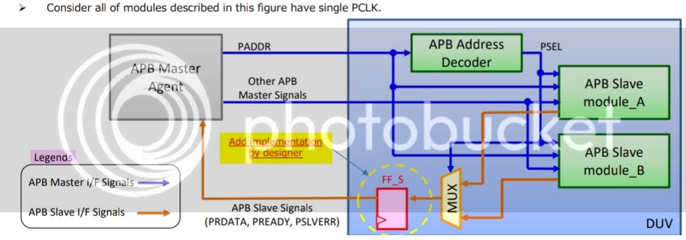
The 1st question is : What is purpose (intention of designer) for flip flop insertion in this design ?
=> As my understanding, I think designer use flip flop to make the Data Stability to Avoid Data Loss. Do we have another intention for this modification ?
The 2nd question is : Do we have any failure operation(bug) case in such modification ?
=> I consider about timing bug. It means that the timing between PENABLE , PSEL input from master (without delay) & response from slave (with delay 1cycle).
PENABLE must still be generated by the APB master so that simpler APB peripheral designs can just detect the “setup” and “access” phases of each transfer by gating together PSEL, PENABLE and PREADY. The access phase might be wrong in this case.
=> Beside that, I cannot think another potential bug for this modification . If you have any idea, please share with me.
The 3rd question is : Could we change the modification method to keep intention of designer & avoid some bug as above ?
=> I do not have any idea for this question. Please share with me your thinking.
I’m so sorry about my English. You can feel so hard to understand what I described in above. Please share any question, thinking . I will try explain any your unclear point.
Thank you,
In reply to thanhnguyen.jg:
You should ask the designer what the intention of the FF is (it switches between the 2 slaves. But is there more behind?
Olease consider this is an UVM forum and not a common design or verification forum.
In reply to chr_sue:
In reply to thanhnguyen.jg:
You should ask the designer what the intention of the FF is (it switches between the 2 slaves. But is there more behind?
Olease consider this is an UVM forum and not a common design or verification forum.
This lab is base on the sample project. We got the request to verify this DUV by UVM. During the project , the design have been updated by designer.
=> Verifier should estimate the potential bug with each modification and create pattern to check it.
That is the reason why I put my question in UVM forum.
In reply to thanhnguyen.jg:
OK, I understood. But what is requested to you is the normal request a verification engineer has to fulfill.
With respect to the FF in the red circle I assume it controls which slave will be selected. My guess is the update in your design is the 2nd slave. Right? And of course you have to make sure slave B is not hiding any bug.
Run all your test first for slave A and then for slabe B.
In reply to thanhnguyen.jg:
Dear All,
I’m learning about UVM for verification. I got the test for verification planning & bug curve. The test is below:
The 1st question is : What is purpose (intention of designer) for flip flop insertion in this design ?
=> As my understanding, I think designer use flip flop to make the Data Stability to Avoid Data Loss. Do we have another intention for this modification ?
The 2nd question is : Do we have any failure operation(bug) case in such modification ?
=> I consider about timing bug. It means that the timing between PENABLE , PSEL input from master (without delay) & response from slave (with delay 1cycle).
PENABLE must still be generated by the APB master so that simpler APB peripheral designs can just detect the “setup” and “access” phases of each transfer by gating together PSEL, PENABLE and PREADY. The access phase might be wrong in this case.
=> Beside that, I cannot think another potential bug for this modification . If you have any idea, please share with me.
The 3rd question is : Could we change the modification method to keep intention of designer & avoid some bug as above ?
=> I do not have any idea for this question. Please share with me your thinking.
I’m so sorry about my English. You can feel so hard to understand what I described in above. Please share any question, thinking . I will try explain any your unclear point.
Thank you,
Instead of answering each of the questions, let me share my inputs in general.
As you can see, the flop at the output is to make sure that outputs are registered.
This ensures 2 things and mostly related:
- the signal gets complete clock cycle as margin from a timing perspective.
So, you can effectively have this signal quite long from a PD perspective.
- if this output is directly used then glitches before the flop will propagate.
These glitches can cause issues in certain cases and in certain cases they don’t.
So, since we don’t know how the output would be used, it is safer to register it.
In some projects, we have put glitch checkers (sub-clock pulses). This is very subjective.
This was done based on Architecture’s team inputs on what signal can cause an issue if they generate glitches.
If you change the design the timing changes. So, timing character changes but overall functionality remains the same.
